Professional USB microscope · Electronics/PCB
USB Microscope for PCB and Electronics Inspection
Inspect solder joints, traces, pads, components, contamination, and rework results with magnified image capture.
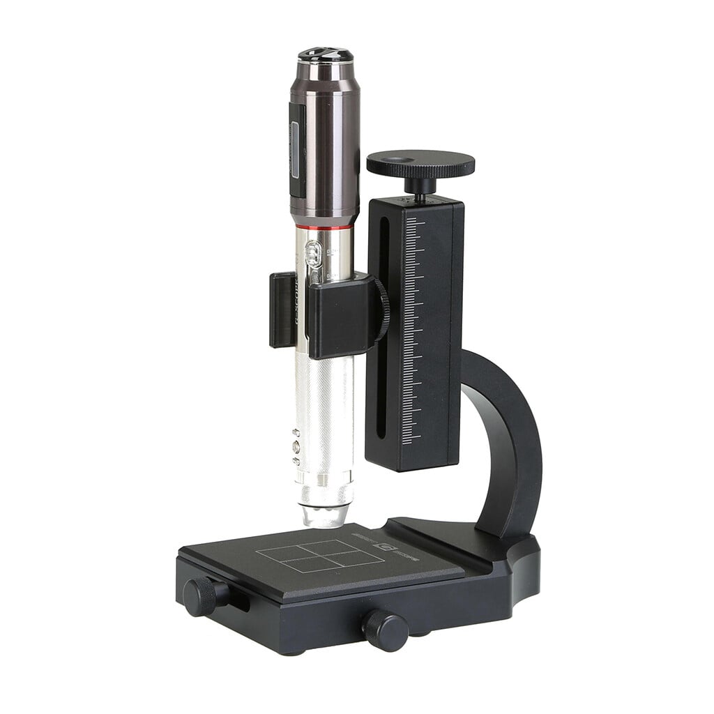

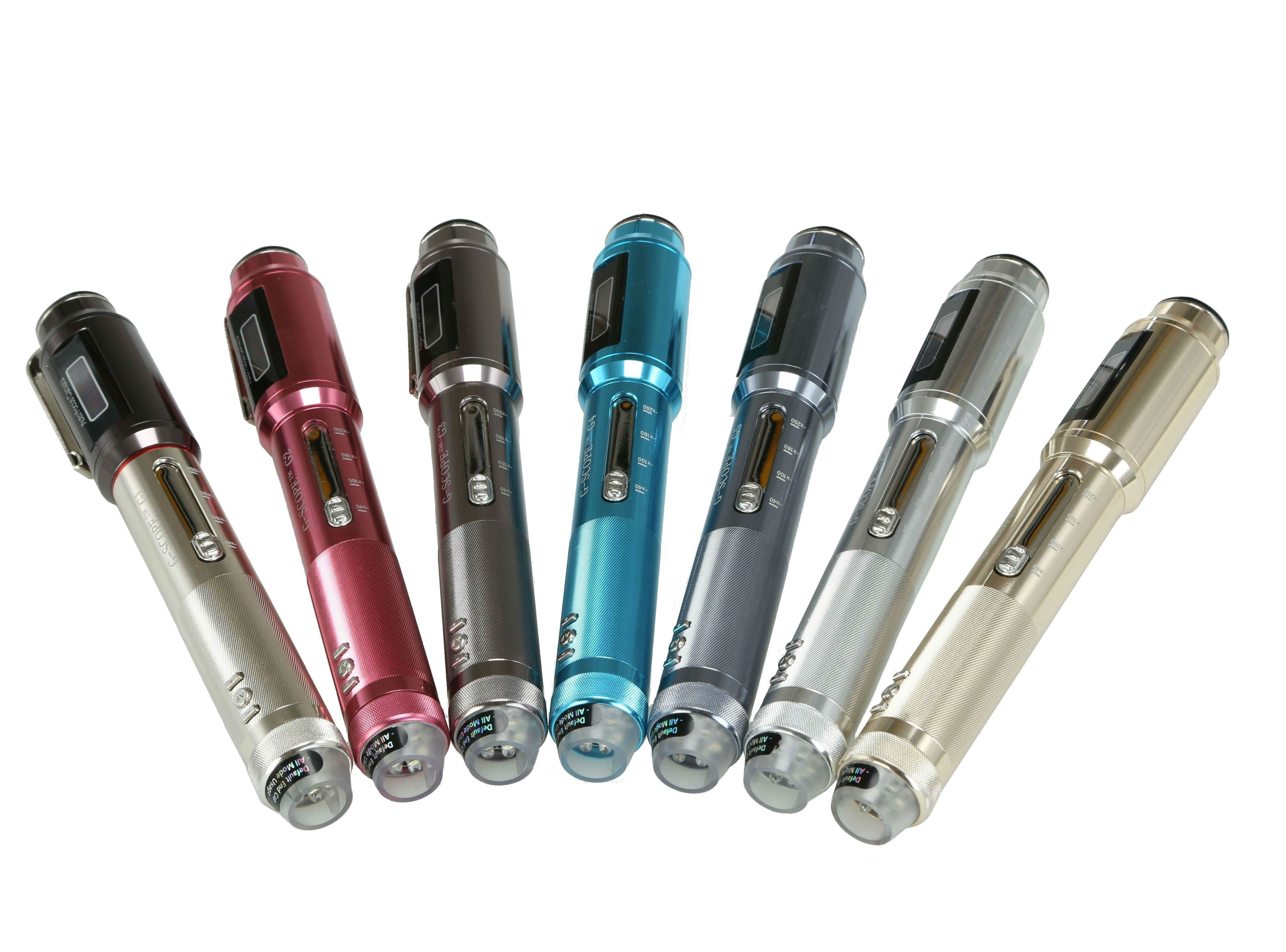
- Four quick magnification levels40x, 100x, 180x and 250x with the general inspection end-cap
- 3Pi narrow-tip end-cap100x access to small or recessed areas that remain in direct line of sight
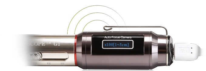
- Quality optics, autofocus + Full HDCorning® Varioptic® liquid lens, photos and 30fps video
- Professional European supportShips from Spain with a two-year warranty
Overview
Smart G-Scope provides magnified, line-of-sight inspection of exposed PCB surfaces such as solder joints, traces, vias, pads, labels, and accessible component leads. What can be resolved depends on magnification, lighting, working distance, and the size and contrast of the feature.
The general inspection end-cap supports 40x, 100x, 180x, and 250x. The smaller-tip 3Pi end-cap works at 100x and can approach small or recessed areas when there is still a clear optical path to the surface.
It can document visible solder bridges, solder balls, residues, alignment, and surface damage for expert review. It cannot see through packages, inspect hidden BGA joints, look around corners, or replace X-ray, cross-sectioning, electrical testing, or certified metrology.
Recommended Smart G-Scope setup
- Use the general inspection end-cap at 40x, 100x, 180x, or 250x for open PCB surfaces.
- Use the narrow-tip 3Pi end-cap at 100x for small or recessed areas only when a direct optical path remains available.
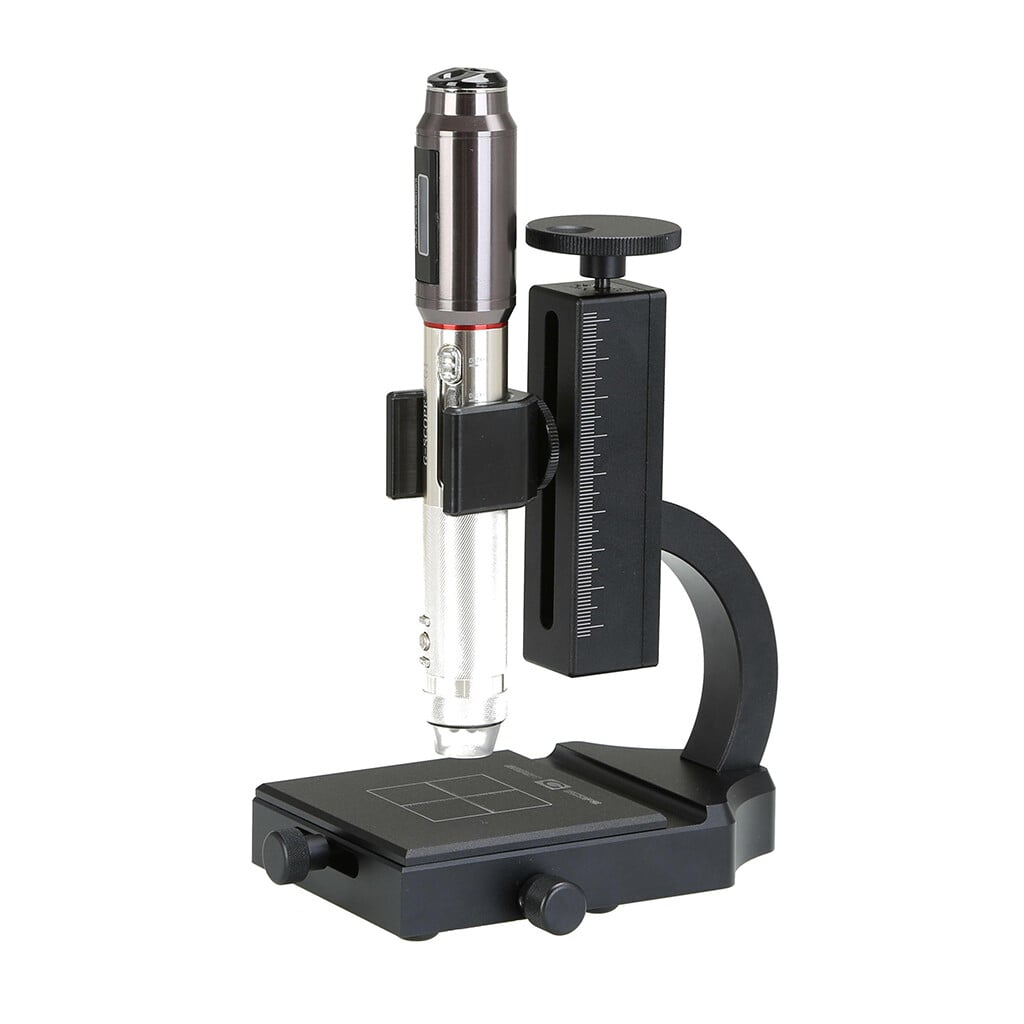
- Use a precision stand for stable board positioning and repeatable images.
- Adjust illumination angle to reduce glare from solder mask and metal pads.
- Use software capture for incoming inspection, rework records, and failure-analysis notes.
- Use a suitable calibrated method instead when measurement accuracy or standards-grade tolerances matter.
What you can observe
- Visible solder bridges, solder balls, surface cracks, wetting appearance, and residues in exposed areas.
- Visible component alignment, package edges, leads, pads, vias, labels, and traces.
- Contamination or handling marks that need quality review.
- Before/after images from rework or process changes.
Typical workflow
- 1Place the board on a stable support and set the inspection area.
- 2Choose lighting that reveals solder shape without harsh reflections.
- 3Capture representative defects with lot, board, and location references.
- 4Compare images across lots or after rework to document process improvements.
Key benefits
- Visual inspection of exposed solder joints, bridges, solder balls, and residues
- Inspection of visible leads, package edges, pads, vias, and optically accessible components
- 100x narrow-tip access with the 3Pi end-cap for suitable recessed areas
- Photo and video documentation for quality, rework, and traceability records
- Portable use at production, rework, service, and R&D benches
Best for
- Electronics QA, rework benches, incoming inspection, R&D labs, and service teams.
- Teams that need fast visual evidence without a full machine-vision station.
Not ideal for
- Inspecting hidden BGA joints, underside terminations, internal board layers, or anything outside direct line of sight.
- Replacing certified metrology where standards-grade tolerances are required.
Image gallery
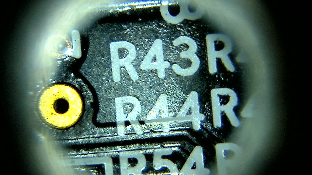
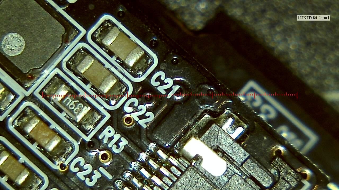
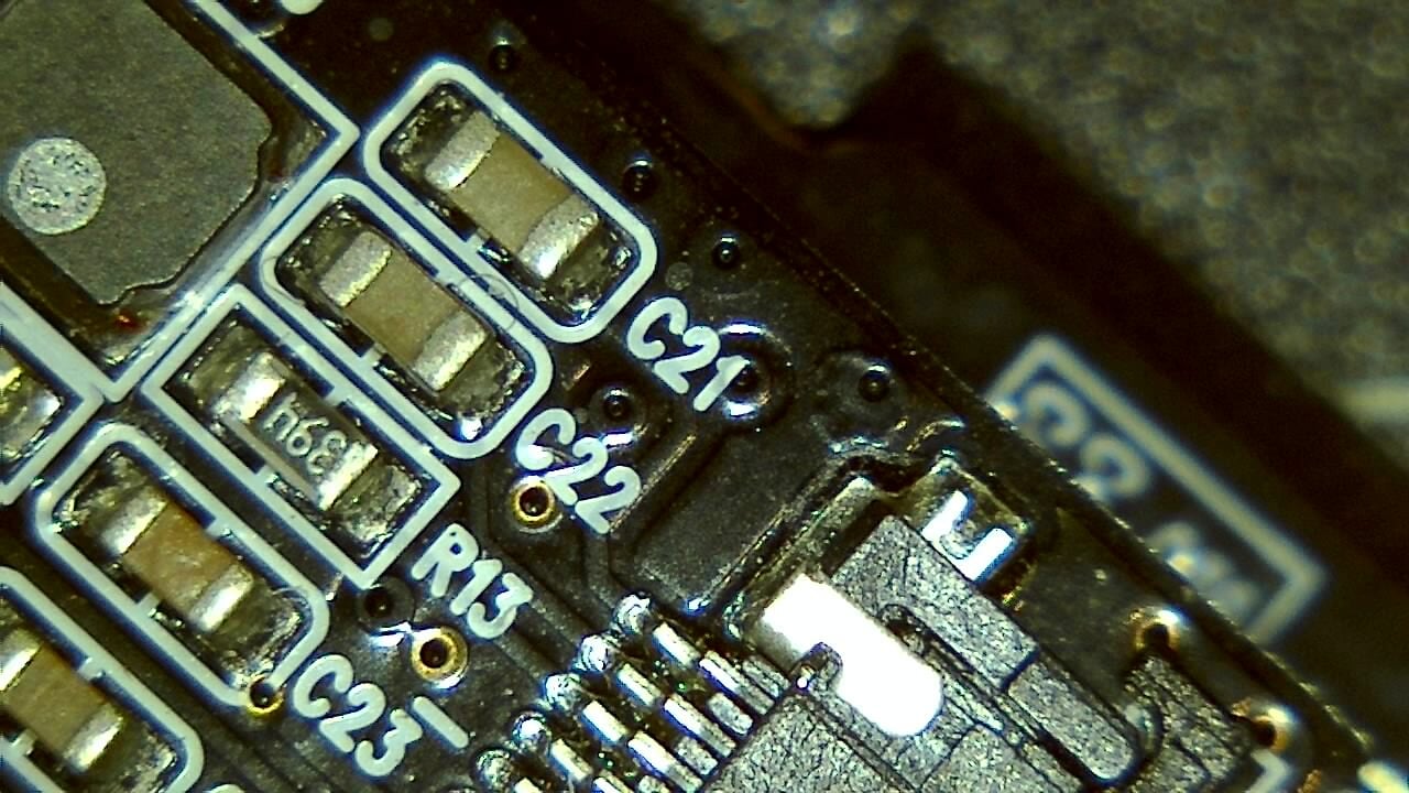
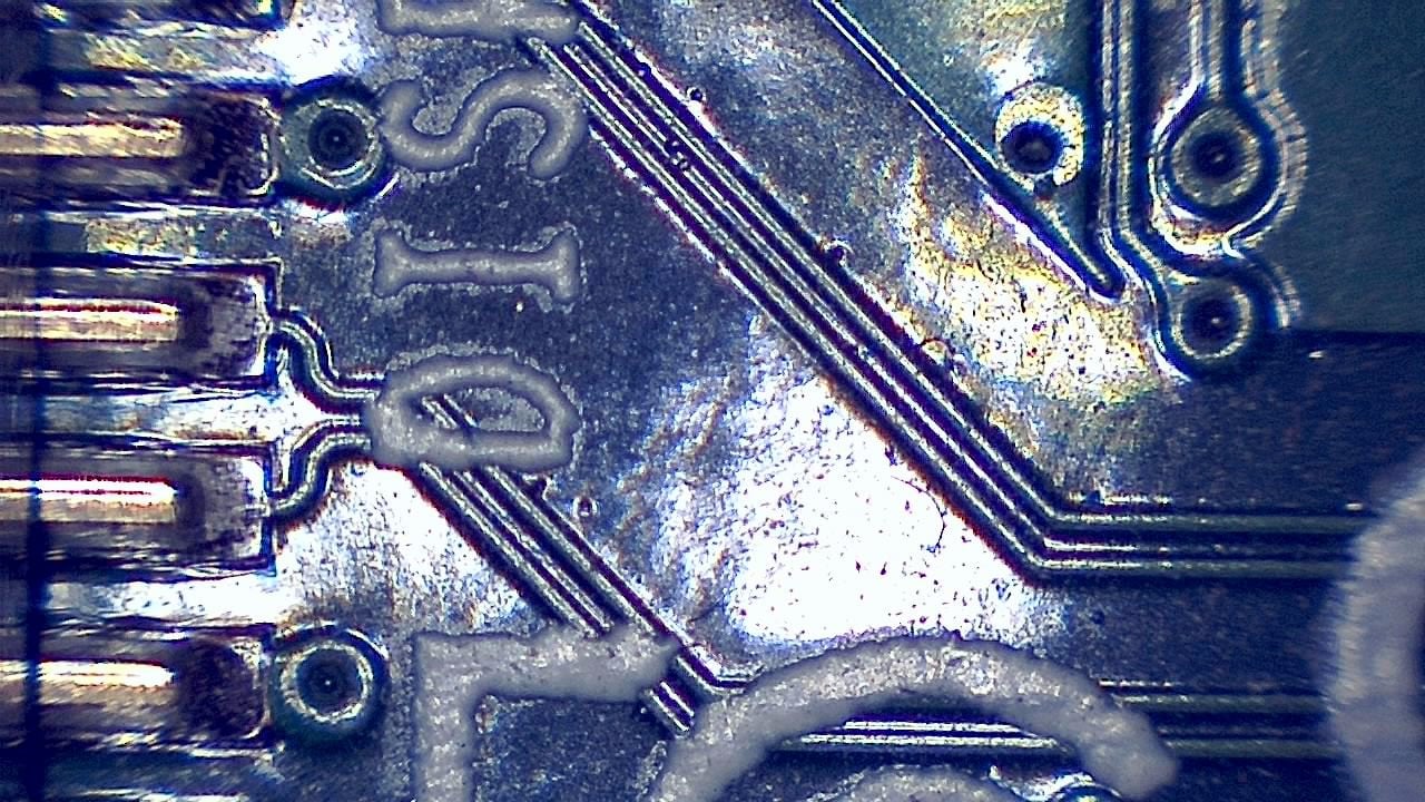
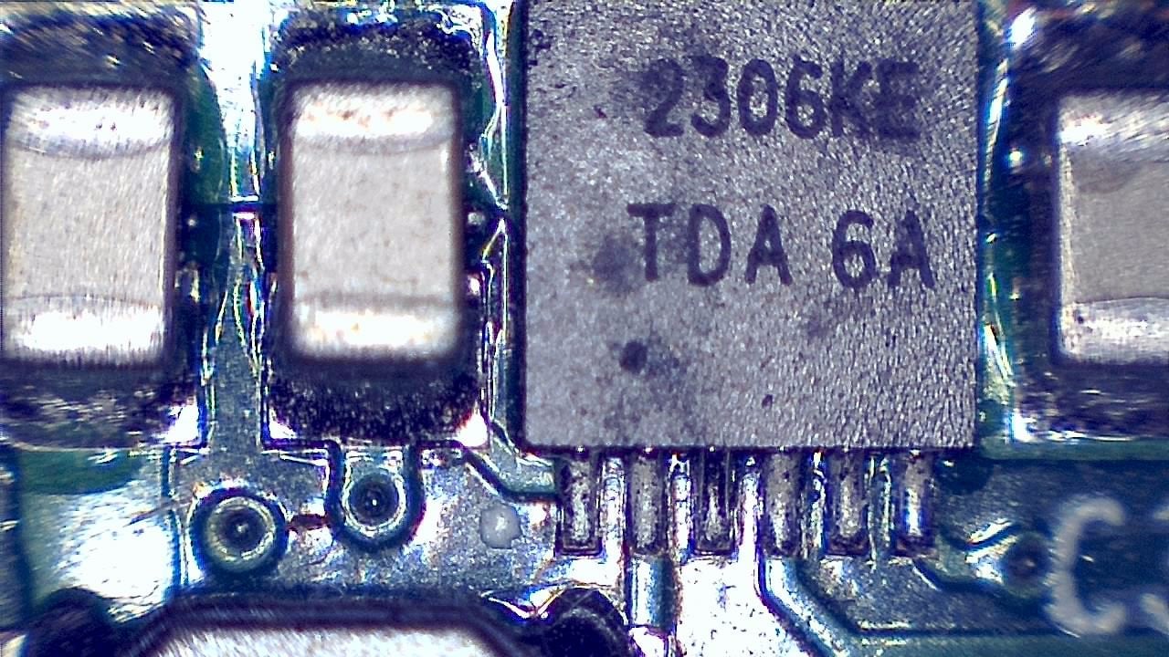
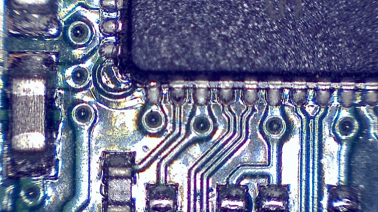
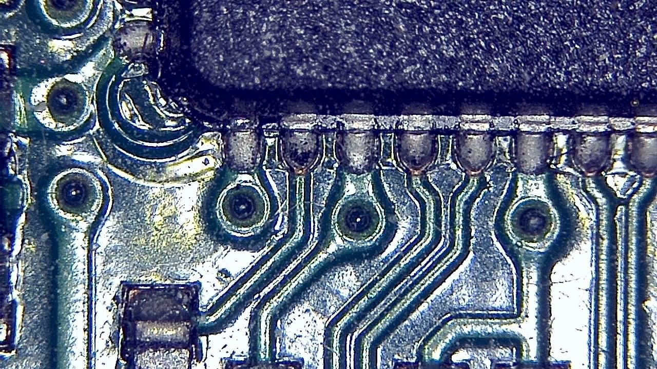
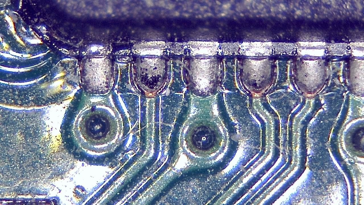
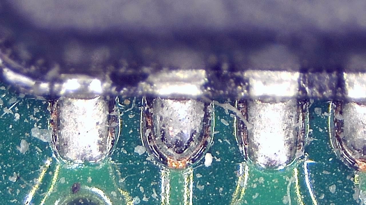
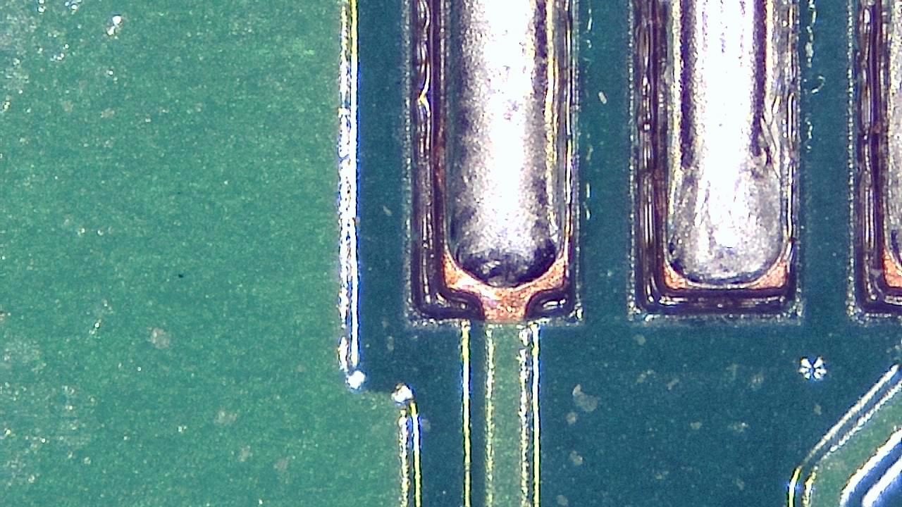
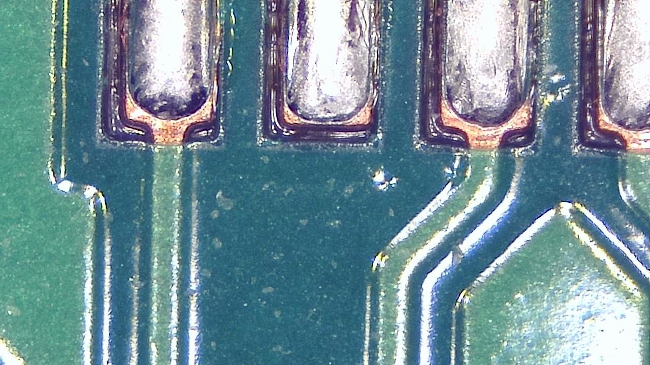
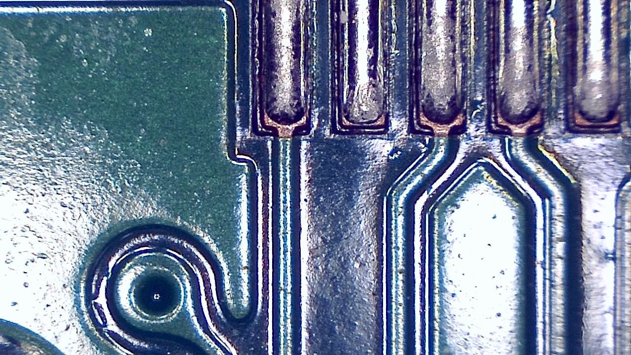
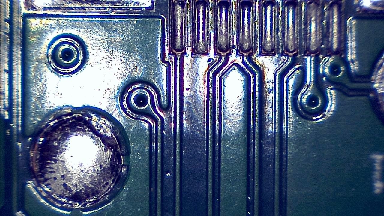
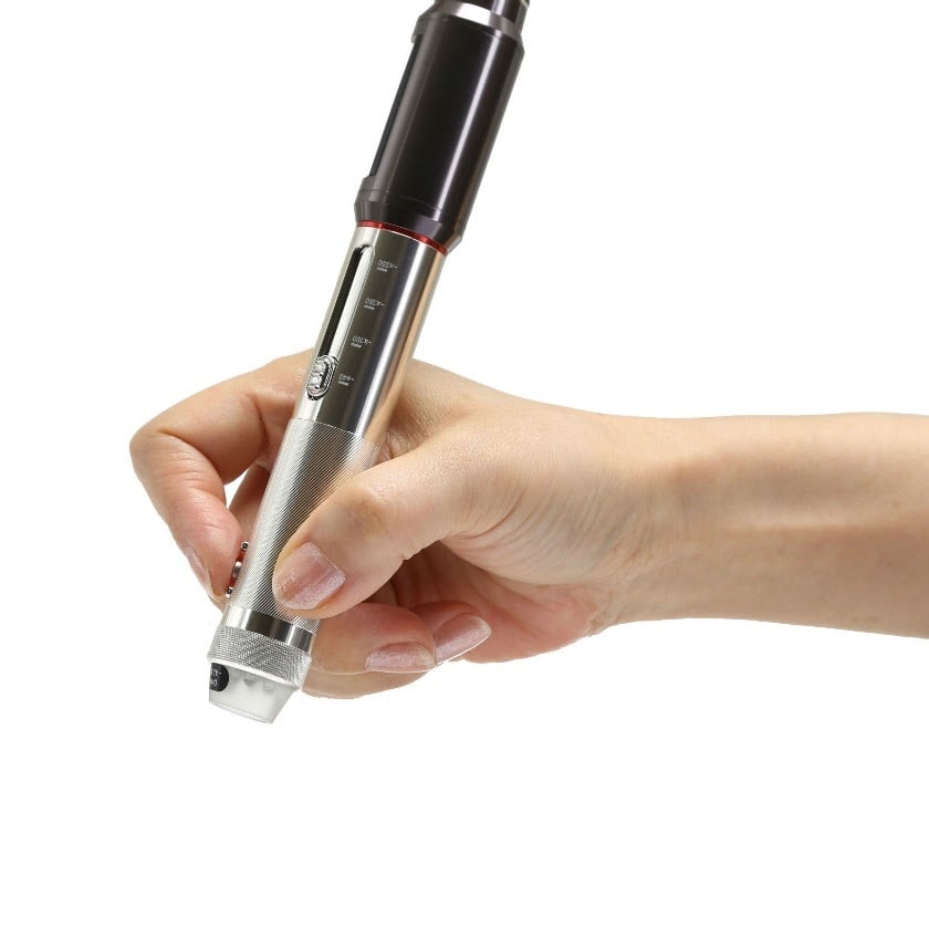
Click any image to enlarge
Practical examples
SMD soldering inspection
On an LED board production line, a quality technician uses Smart G-Scope to visually check exposed solder joints and document suspected bridges before boards move to the next process step.
Field-failure analysis
An engineer photographs a suspicious mark on an exposed solder joint of a returned board, then combines that visual record with electrical testing and other evidence during root-cause analysis.
Limitations & best practices
- Hidden BGA joints, underside terminations, internal layers, and other areas without direct line of sight require X-ray, cross-sectioning, or another suitable technique.
- The 3Pi end-cap provides a smaller 100x tip; it does not see around corners or through components.
- Keep the work area clean to prevent cross-contamination.
- Use a traceable calibrated method when measurement accuracy or standards-grade tolerances matter.
Frequently asked questions
Is a USB microscope useful for PCB inspection?
Yes. It is useful for visual checks of solder joints, components, traces, residues, and rework quality, especially when images need to be documented or shared.
Which stand is recommended for PCB work?
A precision stand is recommended because PCB inspection benefits from stable positioning, repeatable focus, and controlled sample movement.
Can it inspect BGA joints?
It can document optically accessible package surfaces and edges, but it cannot see hidden solder joints beneath a BGA or other bottom-terminated component. Those require X-ray, cross-sectioning, or another suitable inspection method.
What is the 3Pi end-cap for?
The smaller-tip 3Pi end-cap works at 100x and can approach narrow or recessed areas that still have a direct line of sight. It does not see through components or around corners.